3. A Tour of the 100/1000BASE-T1 SFP Hardware
Before learning how to configure and set up the device, let’s examine the device from all sides to understand all of its interfaces and status indicators.
3.1. LED Status Indicators
There are 2 visible LEDs on the device: LED1 and LED2, on the left and right, respectively, when looking into the connector
- LED1: Link Status
OFF = Link Down
GREEN = 1000M
AMBER = 100M
- LED2: RX Activity
OFF = No RX activity
Flashing GREEN = RX at 1000M
Flashing AMBER = RX at 100M
- Other Indications
Both LEDs = BLUE: Device in bootloader
Both LEDs = RED: Device Fatal Error
LED1 = RED: MDIO communication failure
3.2. Connector Interfaces
3.2.1. 100/1000BASE-T1
This SFP module uses an H-MTD connection system with the following pin assignments.

H-MTD Connector Pinout |
||
Pin # |
Label |
Description |
1 |
TRD+ |
Data transmit and receive, positive |
2 |
TRD- |
Data transmit and receive, negative |
For the mating H-MTD connector Reference USCAR-EWCAP Drawing Number 777-U-002-1-Z01
Important
The manufacturing of reliable 1000BASE-T1 cables is complex and requires specialized equipment to insure the electrical characteristics are met to achieve a stable link with acceptable SQI. Modifying these cables or attempting to assemble cables without the proper knowledge and equipment can often lead to problems with establishing a link between two devices.
3.2.2. SFP Pin assignments:
Pin |
Signal |
Pin |
Signal |
|---|---|---|---|
1 |
GND |
11 |
GND |
2 |
TX_FAULT |
12 |
SGMII_RX_C_N |
3 |
TX_DIS |
13 |
SGMII_RX_C_P |
4 |
SDA |
14 |
GND |
5 |
SCL |
15 |
VCC |
6 |
GND |
16 |
VCC |
7 |
RATE_SEL |
17 |
GND |
8 |
LOSS_OF_SIGNAL |
18 |
SGMII_TX_C_P |
9 |
GND |
19 |
SGMII_TX_C_N |
10 |
GND |
20 |
GND |
SFP Module Retention Feature
When the SFP module is inserted into an SFP slot, there is a locking mechanism for retaining the device in the slot. This locking mechanism can be released by the lever with a blue “ICS” label that rests above the H-MTD connector.
3.3. Device Configuration
Unlike many similar products, there are no DIP switches or other mechanical interfaces to configure this SFP module. If used with a RAD-Gigastar, the PHY settings can be changed using neoVI Explorer in configuration screen seen below.
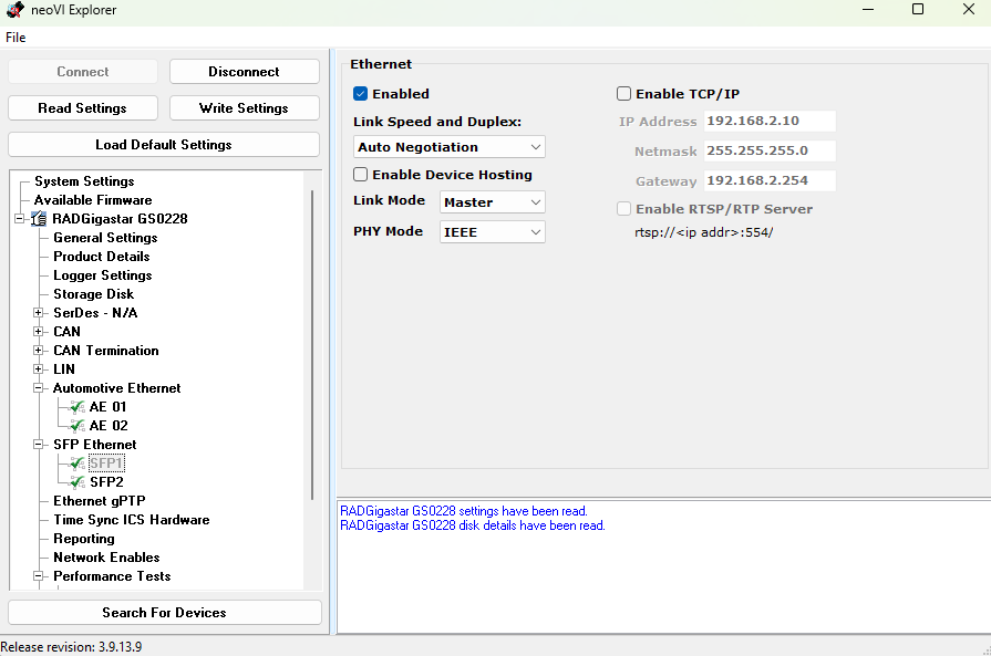
If you are unfamiliar with this screen or the use of RAD-Gigastar, please reference the RAD-Gigastar User Guide
Configurations can also be made using I2C communication to the device and stored in non-volatile memory. The use of I2C for this and other purposes is explained in the next section.
3.4. I2C Communication
I2C communication with the SFP can be accomplished using 1 of 2 methods
Using a SFP host having exposed access to the I2C bus of the SFP module
Host the SFP module in an Intrepid product and use Vehicle Spy or the Intrepid API to send and receive I2C messages.
The following lists the Intrepid products capable of hosting this SFP as well as the I2C networks assigned to each SFP slot within VSPY.
Product |
VSPY I2C Network |
|
RAD-Gigastar |
SFP1 |
I2C 02 |
SFP2 |
I2C 03 |
I2C Addressing
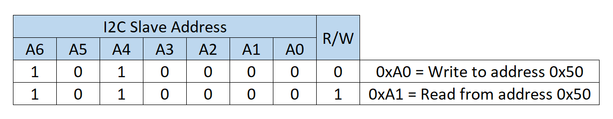
The first byte of an I2C message consists of a 7-bit device address appended with a read/write bit in the least significant position. It is worth pointing out that while I2C is limited to 7-bit device addresses, it is not uncommon for references to be made to 8-bit values that include the read/write bit. For example, below shows how 0xA0 refers to a write to device address 0x50 and 0xA1 refers to a read to that same address.
The SFP responds to the following 4 different I2C addresses
3.4.1. Address 0x50 - Read SFP MSA Table
A read of the MSA table could be done in VSPY with the following message.
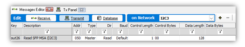
This starts at register 0 and reads the first 128 bytes from the table.
The SFP MSA table is a 512-Byte table of which the contents are defined by SFP specification. The exact table contents are defined in the SFF-8472-Diagnostic_Monitoring_Interface specification.
Value (Hex) |
|||
Byte Index |
Byte Description |
SFP-MV2112-A2 |
SFP-MV2221M-B1 |
Byte 0 |
Identifier |
0x03 |
0x03 |
Byte 1 |
Ext. identifier |
0x04 |
0x04 |
Byte 2 |
Connector |
0xAF |
0xAF |
Byte 3-10 |
Tranceiver |
0x00 |
0x00 |
Byte 11 |
Encoding |
0x00 |
0x00 |
Byte 12 |
BR, Nominal |
0x0A |
0x0A |
Byte 13 |
Rate identifier |
0x00 |
0x00 |
Byte 14-17 |
Link Length (Fiber) |
0x00 |
0x00 |
Byte 18 |
Link Length (Copper) |
0x0A |
0x0A |
Byte 19 |
Link Length (Fiber) |
0x00 |
0x00 |
Byte 20 |
SFP Vendor Name (ASCII) |
0x49 |
0x49 |
Byte 21 |
SFP Vendor Name (ASCII) |
0x6E |
0x6E |
Byte 22 |
SFP Vendor Name (ASCII) |
0x74 |
0x74 |
Byte 23 |
SFP Vendor Name (ASCII) |
0x72 |
0x72 |
Byte 24 |
SFP Vendor Name (ASCII) |
0x65 |
0x65 |
Byte 25 |
SFP Vendor Name (ASCII) |
0x70 |
0x70 |
Byte 26 |
SFP Vendor Name (ASCII) |
0x69 |
0x69 |
Byte 27 |
SFP Vendor Name (ASCII) |
0x64 |
0x64 |
Byte 28 |
SFP Vendor Name (ASCII) |
0x43 |
0x43 |
Byte 29 |
SFP Vendor Name (ASCII) |
0x53 |
0x53 |
Byte 30-35 |
SFP Vendor Name (ASCII) |
0x20 |
0x20 |
Byte 36 |
Transceiver |
0x00 |
0x00 |
Byte 37 |
Vendor OUI |
0x00 |
0x00 |
Byte 38 |
Vendor OUI |
0xFC |
0xFC |
Byte 39 |
Vendor OUI |
0x70 |
0x70 |
Byte 40 |
Vendor PN (ASCII) |
0x53 |
0x53 |
Byte 41 |
Vendor PN (ASCII) |
0x46 |
0x46 |
Byte 42 |
Vendor PN (ASCII) |
0x50 |
0x50 |
Byte 43 |
Vendor PN (ASCII) |
0x2D |
0x2D |
Byte 44 |
Vendor PN (ASCII) |
0x4D |
0x4D |
Byte 45 |
Vendor PN (ASCII) |
0x56 |
0x56 |
Byte 46 |
Vendor PN (ASCII) |
0x32 |
0x32 |
Byte 47 |
Vendor PN (ASCII) |
0x31 |
0x32 |
Byte 48 |
Vendor PN (ASCII) |
0x31 |
0x32 |
Byte 49 |
Vendor PN (ASCII) |
0x32 |
0x31 |
Byte 50 |
Vendor PN (ASCII) |
0x2D |
0x4D |
Byte 51 |
Vendor PN (ASCII) |
0x41 |
0x2D |
Byte 52 |
Vendor PN (ASCII) |
0x32 |
0x42 |
Byte 53 |
Vendor PN (ASCII) |
0x20 |
0x31 |
Byte 54 |
Vendor PN (ASCII) |
0x20 |
0x20 |
Byte 55 |
Vendor PN (ASCII) |
0x20 |
0x20 |
Byte 56 |
Vendor PN (ASCII) |
0x33 |
0x32 |
Byte 57 |
Vendor PN (ASCII) |
0x2E |
0x2E |
Byte 58 |
Vendor PN (ASCII) |
0x30 |
0x30 |
Byte 59 |
Vendor PN (ASCII) |
0x20 |
0x20 |
Byte 60-61 |
Wavelength |
0x00 |
0x00 |
Byte 62 |
Unallocated |
0x00 |
0x00 |
Byte 63 |
CC_BASE |
0xFB |
0x28 |
Byte 64 |
Options |
0x00 |
0x00 |
Byte 65 |
Options |
0x02 |
0x02 |
Byte 66-67 |
BR max,min |
0x00 |
0x00 |
Byte 68 |
Vendor SN (ASCII) |
0x53 |
0x53 |
Byte 69 |
Vendor SN (ASCII) |
0x31 |
0x32 |
Byte 70-73 |
Vendor SN (ASCII) |
xx |
xx |
Byte 74-83 |
Vendor SN (ASCII) |
xx |
xx |
Byte 84 |
Vendor Manufacturer Date (ASCII) |
xx |
xx |
Byte 85 |
Vendor Manufacturer Date (ASCII) |
xx |
xx |
Byte 86 |
Vendor Manufacturer Date (ASCII) |
xx |
xx |
Byte 87 |
Vendor Manufacturer Date (ASCII) |
xx |
xx |
Byte 88 |
Vendor Manufacturer Date (ASCII) |
xx |
xx |
Byte 89 |
Vendor Manufacturer Date (ASCII) |
xx |
xx |
Byte 90 |
Vendor Manufacturer Date (ASCII) |
xx |
xx |
Byte 91 |
Vendor Manufacturer Date (ASCII) |
xx |
xx |
Byte 92 |
Diagnostic Type |
0x00 |
0x00 |
Byte 93 |
Enhanced Options |
0x00 |
0x00 |
Byte 94 |
SFF-8472 Compliance |
0x00 |
0x00 |
Byte 95 |
CC_EXT (8-bit sum of Bytes [64:94]) |
yy |
yy |
Start of the Vendor-Specific Field |
|||
Byte 96 |
Reserved for future use |
||
Byte 97 |
|||
Byte 98-126 |
ICS_RESERVED |
0xFF |
0xFF |
Byte 127 |
Reserved for future use |
||
ICS_I2C_SFP_SETTINGS
Byte 96 of the MSA table holds the non-volatile PHY configuration and a couple SFP pin support flags. When the PHY settings are changed via I2C or neoVI Explorer, the new settings are saved to non-volatile memory to ensure the device boots back up into this state/configuration on next plug-in.
Value = 0 |
Value = 1 |
||
Bit 0 |
Link Speed |
100Mbps |
1000Mbps |
Bit 1 |
Reserved |
X |
X |
Bit 2 |
Marvell Link Operation Mode |
Legacy |
IEEE |
Bit 3 |
Link Mode |
Master |
Slave |
Bit 4 |
Auto Link Mode |
Disabled |
Enabled |
Bit 5 |
Auto Negotiation |
Enabled |
Disabled |
Bit 6 |
Support Rate Select |
Enabled |
Disabled |
Bit 7 |
Support TX Disable |
Enabled |
Disabled |
3.4.2. Address 0x51 - SFP Diagnotic Monitoring Interface
This functionality is not currently supported and will respond with 0xFF when read.
3.4.3. Address 0x40 - I2C MDIO Bridge
The registers of the PHY can be read and written using address 0x40.
Writing to an MDIO Register
Writing to a register is done by sending the following sequence of bytes to the SFP over I2C.
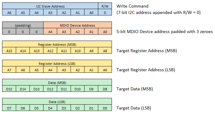
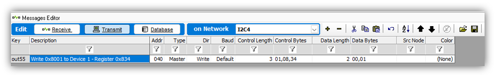
This can be done in Vehicle Spy by sending an I2C message to the SFP hosted in a RAD-Gigastar.
The message editor creates the first byte using the address and R/W bit.
There are 3 “Control Bytes” consisting of the MDIO Address and the target address of the register.
The 2 “Data Bytes” is the value to be written to the target register.
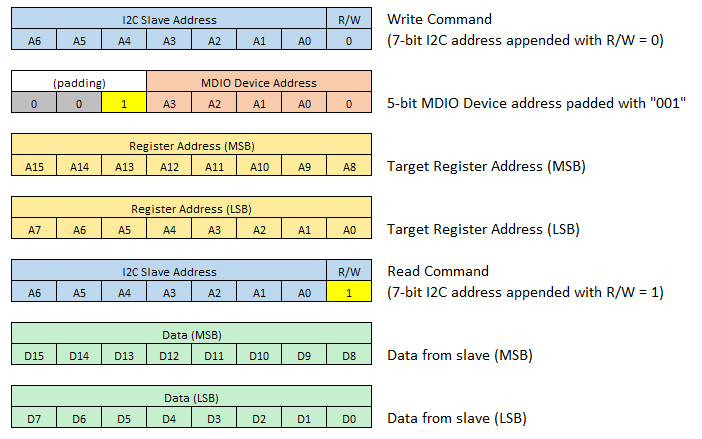
Reading an MDIO Register
Reading an MDIO register over I2C is not an atomic transaction but requires a write command followed by a read command.
Step 1:
The address of the register to be read must first be sent to the slave in a write command. This is done by padding the MDIO device address with “001” (instead of “000”) which tells the slave that there is no data being written to a register, but to use the received address when responding to the next read command.
Step 2:
A read command is sent to the slave and a response is received with the contents of the register address written in step 1.
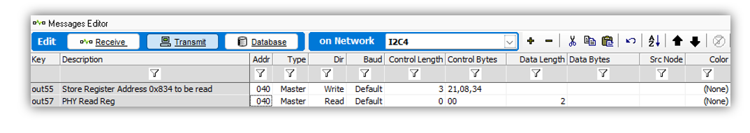
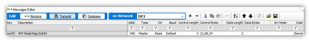
Sending the following messages will read the contents of register 0x0834.
Note
The MDIO Device Address is padded with “001” to indicate that it is not a register write command, but a command to store the register address for the next read command.
The read command has no control bytes
The number of data bytes in the read command determines how long the master will continue sending the clock to the slave and receive data.
Alternative shortcut to reading an MDIO Register in Vehicle Spy
While there are valid reasons why a read from a device over I2C requires 2 operations, an I2C register read can be accomplished with a single message in Vehicle Spy. The following message in Vehicle Spy will generate the same 2 messages on the I2C bus as the previous I2C write example.
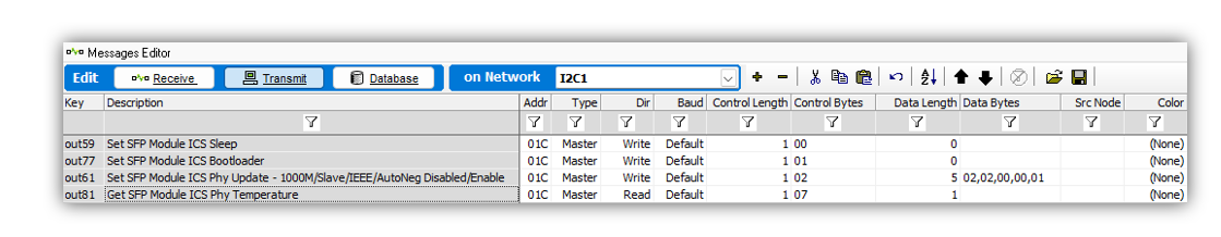
3.4.4. Address 0x1C - Intrepid Device Commands
Writing to address 0x1C with one of the following control byte values can be used to change the PHY configuration, mode of operation, as well as read back information such as PHY temperature and firmware version.
Control Byte |
Command |
||
Write Commands |
0 |
Enter Lower Power Mode |
Device will remain in low power until I2C message matching any of the 4 supported i2c slave addresses. |
1 |
Jump to Bootloader |
SFP remains in bootloader expecting firmware update. Exit via power cycle. |
|
2 |
PHY Configuration Command |
The PHY configuration can be changed by sending this control byte value accompanied with 5 data bytes |
|
3 |
TC10 Wakeup |
(88Q2221M Only) |
|
4 - 6 |
Reserved |
||
Read Commands |
7 |
Read PHY Temperature |
Value in Celsius |
8 |
Read Major Firmware Version |
||
9 |
Read Minor Firmware Version |
||
All other Control Byte values are reserved |
|||
Data Byte Encoding for 0x1C PHY Configuration Command
Data Bytes |
PHY Setting |
Data Byte Value |
|
Byte 1 |
Link Speed |
0x01 = 100Mbps |
All other values default to 100Mbps |
0x02 = 1000Mbps |
|||
Byte 2 |
Link Mode |
0x01 = Master |
All other values default to Slave |
0x02 = Slave |
|||
0x03 = Auto |
|||
Byte 3 |
Op Mode |
0x00 = IEEE |
All other values default to IEEE |
0x01 = Legacy |
|||
Byte 4 |
Auto-Negotiation |
0bxxxxxxx0 = Disabled |
LSb state enables/disabled feature |
0bxxxxxxx1 = Enabled |
|||
Byte 5 |
PHY Enable/Disable |
0bxxxxxxx0 = Disabled |
LSb state enables/disabled PHY |
0bxxxxxxx1 = Enabled |
The following shows example messages for various 0x1C commands.