
Figure 1 - the neoVI block diagram (click for larger image)
Theory of Operation - neoVI
Main
Applies to
neoVI Blue
This section details the theory-of-operation of the neoVI device. A block diagram of the device is shown in figure 1 below.
The neoVI device consists of three independent µControllers which have a total of 20 MIPS (millions of instructions per second) of processing power. This processing power can read messages from 9 independent networks. After reading the messages the neoVI can do one or all of the following things: 1) send them to the PC via RS232 or USB, 2) process the message, or 3) store the message in onboard storage.
The functionality of the neoVI is based on its firmware. All three of the µControllers in the neoVI device have field upgradeable firmware. This means the neoVI device can be updated with new functionality at anytime in the future.
The following topics explain the diagram further: 1) Main 51 µController, 2) Main PIC µController, 3) CAN Networks, 4) LBCC Protocol IC, and 5) ISO/J PIC µController section.
Figure 1 - the neoVI block diagram (click for
larger image)
The Main 51 µController (figure 2) is responsible for collecting messages from the Main PIC µController and processing them. Normally, when neoVI is used as a PC interface this means sending them to the PC via USB or RS232. It also could store the messages on it's MMC (multimedia card storage device). It could also process the messages and do something such as transmit a response or change a general purpose IO bit.
The RS232 port is capable of 115.2 kb, 57.6 kb, 38.4 kb, 28.8 kb, 19.2 kb, 9600 bps, and 4800 bps baud rates. It includes RS232 control lines for hardware handshaking (RTS/CTS) and DTR acting as a DCE (Data Communication Equipment) device.
The USB port supports USB 1.1 full speed 12 Mega-Bits per second. The device is software programmable to use either Bulk only or Isochronous in/bulk out transfers.
The neoVI device defaults to 56k Baud RS232 communication on power up. The communication can then be changed by the host software by sending commands on USB or RS232.
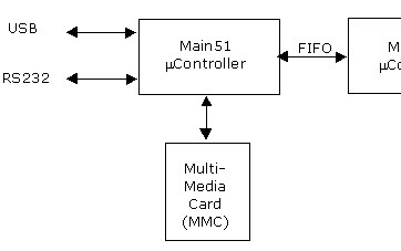
Figure 2 - The Main 51 µController
The Main PIC µController is the heart of the Vehicle network functions. Its job is to read network messages from the specific subsections, timestamp them and send them to the Main 51 µController.
The Main PIC µController is directly responsible for the MISC 1 and MISC 2 signals, the J1708 protocol, and configuration of the LBCC and CAN controllers. As the owner of the timestamp clock, the Main PIC generates the time-stamp clock for the DAQ pacer functionality. It also owns the trigger signals for J1708, Ford SCP (LBCC), and all of the CAN networks.
The Main PIC µController is protected by a internal watchdog timer and controls the reset lines for all of the other circuits.
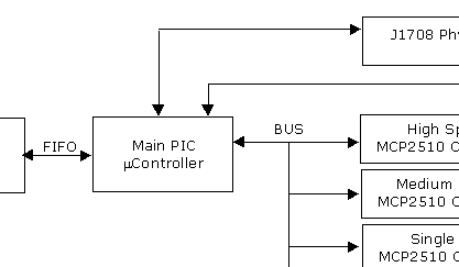
Figure 3 - The Main PIC µController
neoVI has four independent CAN networks. The CAN protocol IC is the MCP2510 IC from Microchip Technology. Each protocol chip, is connected to the appropriate physical layer for that CAN network. All status and control signals for each physical layer are mapped to internal µController pins. This allows complete software control of the CAN functionality.
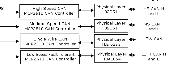
Figure 4 - The neoVI CAN Networks
The LBCC protocol is a protocol IC from Visteon which performs the J1850 PWM Ford SCP protocol. It supports a programmable function id table with 31 locations, a programmable network address, and two programmable function read data registers.
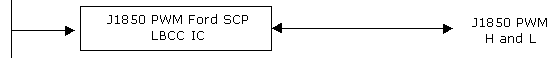
Figure 5- The neoVI LBCC interface
The ISO/J PIC µController main functionality is to generate the J1850 VPW and ISO/UART protocols. Other responsibilities include the following: 1) LED Control, 2) Real-Time Clock Interfacing, 3) On-board Temperature Sensor Interfacing, and 4) MISC signals 3 through 7.
The J1850 VPW software is software controlled peripheral based VPW generation. This means that the ISO/J PIC µController uses a timing peripheral to generate and receive variable pulse width (VPW) waveforms. This allows the neoVI device to create faults and analyze VPW waveforms that would not be possible with other protocol ICs. It also allows support of different in-frame responses which cause incompatibilities between J1850 VPW protocol ICs.
The ISO/UART section is very flexible. The K and L lines have software controlled transmit enable lines allowing many different variants of UART or ISO9141 communications including: Tx on L Rx on K; Tx and Rx on K; Tx on K and L and Rx on K.
The MISC signals contain four 10 bit analog inputs and one external wake-up input.
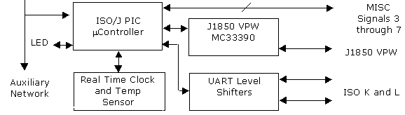
Figure 6 - The ISO/J PIC µController Section
| neoVI Documentation - (C) Copyright 2000-2020 Intrepid Control Systems, Inc. |
Last Update: Thursday, July 09, 2009