3. A Tour of the MultiGBASE-T1 SFP Hardware
Before learning how to configure and set up the device, let’s examine the device from all sides to understand all of its interfaces and status indicators.
3.1. LED Status Indicators
There are 2 visible LEDs on the device: LED1 and LED2, on the left and right, respectively, when looking into the connector
Link Speed |
Amber |
2.5G or 5G |
Green |
10G |
Link Status |
Amber LED |
Off |
Link Inactive |
Solid |
Link Active |
||
Flashing |
RX/TX activity |
||
Red LED |
Flashing |
Malformed Frame |
|
Solid |
MDIO Com Failure |
||
Both Red: Device Fatal Error |
|||
Both Blue: Device in bootloader |
|||
3.2. Connector Interfaces
3.2.1. Automotive Ethernet
This SFP module uses an H-MTD connection system with the following pin assignments.
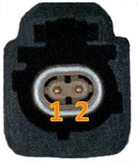
H-MTD Connector Pinout |
||
Pin # |
Label |
Description |
1 |
TRD+ |
Data transmit and receive, positive |
2 |
TRD- |
Data transmit and receive, negative |
For the mating H-MTD connector Reference USCAR-EWCAP Drawing Number 777-U-002-1-Z01
Important
The manufacturing of reliable Automotive Ethernet cables for 1Gbps speeds and above is complex and requires specialized equipment to insure the electrical characteristics are met to achieve a stable link with acceptable SQI. Modifying these cables or attempting to assemble cables without the proper knowledge and equipment can often lead to problems with establishing a link between two devices.
SFP Module Retention Feature
When the SFP module is inserted into an SFP slot, there is a locking mechanism for retaining the device in the slot. This locking mechanism can be released by the lever with a blue “ICS” label that rests above the H-MTD connector.
3.2.2. SFP+ Pin assignments:
PIN |
MultiG |
PIN |
MultiG |
|
1 |
GND |
11 |
GND |
|
2 |
TX_FAULT |
12 |
SFI_RX_C_N |
|
3 |
TX_DIS |
13 |
SFI_RX_C_P |
|
4 |
SDA |
14 |
GND |
|
5 |
SCL |
15 |
VCC |
|
6 |
GND |
16 |
VCC |
|
7 |
RATE_SELECT0 |
17 |
GND |
|
8 |
LOSS_OF_SIGNAL |
18 |
SFI_TX_C_P |
|
9 |
RATE_SELECT1 |
19 |
SFI_TX_C_N |
|
10 |
GND |
20 |
GND |
3.3. Device Configuration
Unlike many similar products, there are no DIP switches or other mechanical interfaces to configure this SFP module. If used with a RAD-Gigastar, the PHY settings can be changed using neoVI Explorer in configuration screen seen below.
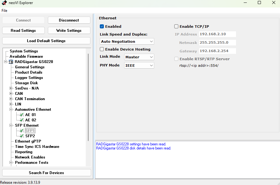
If you are unfamiliar with this screen or the use of RAD-Gigastar, please reference the RAD-Gigastar User Guide
Configurations can also be made using I2C communication to the device and stored in non-volatile memory. The use of I2C for this and other purposes is explained in the next section.
3.4. I2C Communication
I2C communication with the SFP can be accomplished using 1 of 2 methods
Using a SFP host having exposed access to the I2C bus of the SFP module
Host the SFP module in an Intrepid product and use Vehicle Spy or the Intrepid API to send and receive I2C messages.
The following lists the Intrepid products capable of hosting this SFP as well as the I2C networks assigned to each SFP slot within VSPY.
Product |
VSPY I2C Network |
|
RAD-Gigastar |
SFP1 |
I2C 02 |
SFP2 |
I2C 03 |
I2C Addressing
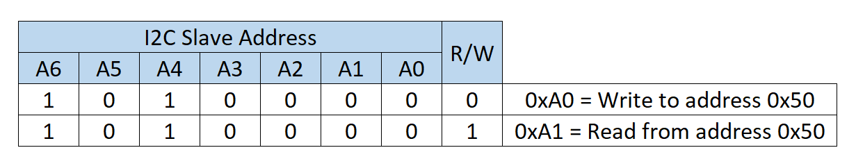
The first byte of an I2C message consists of a 7-bit device address appended with a read/write bit in the least significant position. It is worth pointing out that while I2C is limited to 7-bit device addresses, it is not uncommon for references to be made to 8-bit values that include the read/write bit. For example, below shows how 0xA0 refers to a write to device address 0x50 and 0xA1 refers to a read to that same address.
The SFP responds to the following 4 different I2C addresses
3.4.1. Address 0x50 - Read SFP MSA Table
The SFP MSA table is a 512-Byte table of which the contents are defined by SFP specification. The exact table contents are defined in the SFF-8472-Diagnostic_Monitoring_Interface specification.
MSA (Multi Source Agreement)
MSA stands for Multi Source Agreement. This is an agreement between multiple manufacturers on the standards for a given product. It is intended to ensure common functionality and operability across different suppliers and manufacturers.
A read of the MSA table could be done in VSPY with the following message.
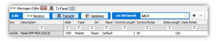
This starts at register 0 and reads the first 128 bytes from the table.
Byte Index |
Byte Description |
Value (Hex) |
|---|---|---|
Byte 0 |
Identifier |
0x03 |
Byte 1 |
Ext. identifier |
0x04 |
Byte 2 |
Connector |
0xAF |
Byte 3-10 |
Tranceiver |
0x00 |
Byte 11 |
Encoding |
0x00 |
Byte 12 |
BR, Nominal |
0x64 |
Byte 13 |
Rate identifier |
0x00 |
Byte 14-17 |
Link Length (Fiber) |
0x00 |
Byte 18 |
Link Length (Copper) |
0x0F |
Byte 19 |
Link Length (Fiber) |
0x00 |
Byte 20 |
SFP Vendor Name (ASCII) |
0x49 |
Byte 21 |
SFP Vendor Name (ASCII) |
0x6E |
Byte 22 |
SFP Vendor Name (ASCII) |
0x74 |
Byte 23 |
SFP Vendor Name (ASCII) |
0x72 |
Byte 24 |
SFP Vendor Name (ASCII) |
0x65 |
Byte 25 |
SFP Vendor Name (ASCII) |
0x70 |
Byte 26 |
SFP Vendor Name (ASCII) |
0x69 |
Byte 27 |
SFP Vendor Name (ASCII) |
0x64 |
Byte 28 |
SFP Vendor Name (ASCII) |
0x43 |
Byte 29 |
SFP Vendor Name (ASCII) |
0x53 |
Byte 30-35 |
SFP Vendor Name (ASCII) |
0x20 |
Byte 36 |
Transceiver |
0x00 |
Byte 37 |
Vendor OUI |
0x00 |
Byte 38 |
Vendor OUI |
0xFC |
Byte 39 |
Vendor OUI |
0x70 |
Byte 40 |
Vendor PN (ASCII) |
0x53 |
Byte 41 |
Vendor PN (ASCII) |
0x46 |
Byte 42 |
Vendor PN (ASCII) |
0x50 |
Byte 43 |
Vendor PN (ASCII) |
0x2D |
Byte 44 |
Vendor PN (ASCII) |
0x4D |
Byte 45 |
Vendor PN (ASCII) |
0x56 |
Byte 46 |
Vendor PN (ASCII) |
0x33 |
Byte 47 |
Vendor PN (ASCII) |
0x32 |
Byte 48 |
Vendor PN (ASCII) |
0x34 |
Byte 49 |
Vendor PN (ASCII) |
0x34 |
Byte 50 |
Vendor PN (ASCII) |
0x2d |
Byte 51 |
Vendor PN (ASCII) |
0x41 |
Byte 52 |
Vendor PN (ASCII) |
0x31 |
Byte 53 |
Vendor PN (ASCII) |
0x20 |
Byte 54 |
Vendor PN (ASCII) |
0x20 |
Byte 55 |
Vendor PN (ASCII) |
0x20 |
Byte 56 |
Vendor PN (ASCII) |
0x33 |
Byte 57 |
Vendor PN (ASCII) |
0x2e |
Byte 58 |
Vendor PN (ASCII) |
0x33 |
Byte 59 |
Vendor PN (ASCII) |
0x20 |
Byte 60-61 |
Wavelength |
0x00 |
Byte 62 |
Unallocated |
0x00 |
Byte 63 |
CC_BASE |
0x04 |
Byte 64 |
Options |
0x00 |
Byte 65 |
Options |
0x02 |
Byte 66-67 |
BR max,min |
0x00 |
Byte 68 |
Vendor SN (ASCII) |
0x53 |
Byte 69 |
Vendor SN (ASCII) |
0x34 |
Byte 70-73 |
Vendor SN (ASCII) |
xx |
Byte 74-83 |
Vendor SN (ASCII) |
xx |
Byte 84 |
Vendor Manufacturer Date (ASCII) |
xx |
Byte 85 |
Vendor Manufacturer Date (ASCII) |
xx |
Byte 86 |
Vendor Manufacturer Date (ASCII) |
xx |
Byte 87 |
Vendor Manufacturer Date (ASCII) |
xx |
Byte 88 |
Vendor Manufacturer Date (ASCII) |
xx |
Byte 89 |
Vendor Manufacturer Date (ASCII) |
xx |
Byte 90 |
Vendor Manufacturer Date (ASCII) |
xx |
Byte 91 |
Vendor Manufacturer Date (ASCII) |
xx |
Byte 92 |
Diagnostic Type |
0x00 |
Byte 93 |
Enhanced Options |
0x00 |
Byte 94 |
SFF-8472 Compliance |
0x00 |
Byte 95 |
CC_EXT (8-bit sum of Bytes [64:94]) |
yy |
Start of the Vendor-Specific Field |
||
Byte 96 |
MDIO Bridge I2C Address |
|
Byte 97 |
Persistent Settings (table) |
|
Byte 98 |
Status Bits (table) |
|
Byte 99 |
PHY SerDes Link Speed (table) |
|
Byte 100-103 |
ICS_RESERVED |
0xFF |
Byte 104 |
bit 0: TC10 sleep active (inverted) |
|
bits 7:1: Reserved |
||
Byte 105-109 |
ICS_RESERVED |
0xFF |
Byte 110-125 |
PCB Serial Number |
|
Byte 126 |
Bootloader |
|
Value of 0xAA indicated the device is in the bootloader. |
||
Byte 127 |
Vendor Overrides: |
|
bit 0: I2C MDIO bridge address override flag (inverted) |
||
bit 1: Soft options override flag (inverted) |
||
Persistent Settings
Byte 97 of the MSA table holds the non-volatile PHY configuration and a couple SFP pin support flags. When the PHY settings are changed via I2C or neoVI Explorer, the new settings are saved to non-volatile memory to ensure the device boots back up into this state/configuration on next plug-in.
Value = 0 |
Value = 1 |
||
Bits 2:0 |
Reserved |
X |
X |
Bit 3 |
Link Mode |
Master |
Slave |
Bit 4 |
Auto Link Mode |
Disabled |
Enabled |
Bit 5 |
Reserved |
X |
X |
Bit 6 |
Support Rate Select |
Enabled |
Disabled |
Bit 7 |
Support TX Disable |
Enabled |
Disabled |
Byte 98 Status Bits
Bit 0: |
TC10 enabled |
|
Bit 1: |
MACsec enabled |
|
Bits 3:2: |
Link Speed |
0b00 = Reserved |
0b01 = 2.5G |
||
0b10 = 5G |
||
0b11 = 10G |
||
Bits 7:4: |
Reserved |
|
PHY SerDes Link Speed
Auto |
0x00 |
2500BASE-X |
0x01 |
2.5GBASE-X |
0x02 |
5000BASE-R |
0x03 |
5GBASE-R |
0x04 |
10GBASE-R |
0x05 |
5G-USXGMII |
0x06 |
10G-USXGMII |
0x07 |
3.4.2. Address 0x51 - SFP Diagnotic Monitoring Interface
This functionality is not currently supported and will respond with 0xFF when read.
3.4.3. Address 0x40 - I2C MDIO Bridge
The registers of the PHY can be read and written using address 0x40.
Writing to an MDIO Register
Writing to a register is done by sending the following sequence of bytes to the SFP over I2C.
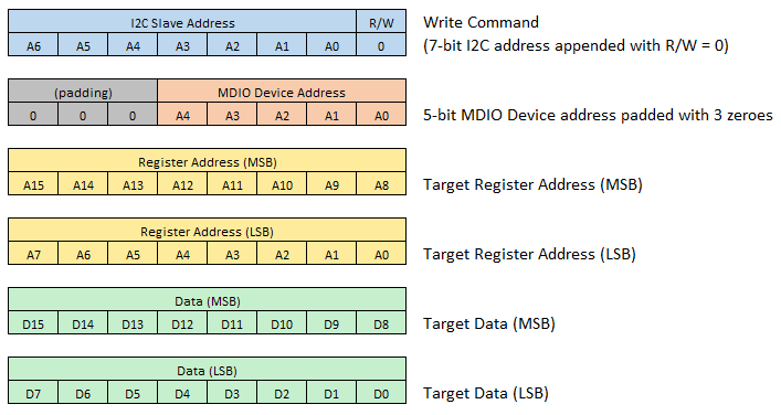
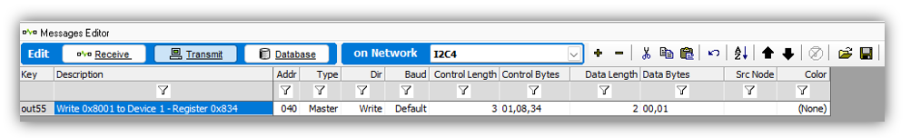
This can be done in Vehicle Spy by sending an I2C message to the SFP hosted in a RAD-Gigastar.
The message editor creates the first byte using the address and R/W bit.
There are 3 “Control Bytes” consisting of the MDIO Address and the target address of the register.
The 2 “Data Bytes” is the value to be written to the target register.
Reading an MDIO Register
Reading an MDIO register over I2C is not an atomic transaction but requires a write command followed by a read command.
Step 1:
The address of the register to be read must first be sent to the slave in a write command. This is done by padding the MDIO device address with “001” (instead of “000”) which tells the slave that there is no data being written to a register, but to use the received address when responding to the next read command.
Step 2:
A read command is sent to the slave and a response is received with the contents of the register address written in step 1.
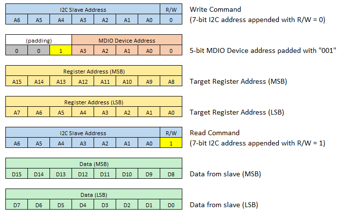
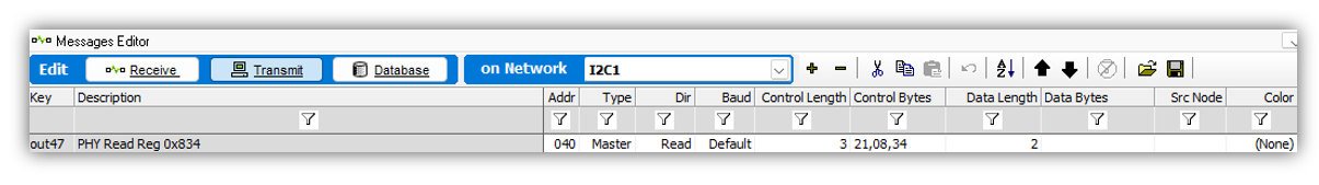
Sending the following messages will read the contents of register 0x0834.
Note
The MDIO Device Address is padded with “001” to indicate that it is not a register write command, but a command to store the register address for the next read command.
The read command has no control bytes
The number of data bytes in the read command determines how long the master will continue sending the clock to the slave and receive data.
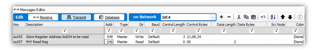
Alternative shortcut to reading an MDIO Register in Vehicle Spy
While there are valid reasons why a read from a device over I2C requires 2 operations, an I2C register read can be accomplished with a single message in Vehicle Spy. The following message in Vehicle Spy will generate the same 2 messages on the I2C bus as the previous I2C write example.
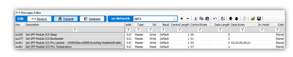
3.4.4. Address 0x1C - Intrepid Device Commands
Writing to address 0x1C with one of the following control byte values can be used to change the PHY configuration, mode of operation, as well as read back information such as PHY temperature and firmware version.
The SFP-MV2112 does not support MACsec or TC10.
Any MACsec or TC10 commands in the following table are not supported by the SFP-MV2112.
Control Byte |
Command Type |
Command |
||
0 |
Write |
Enter Lower Power Mode |
Device will remain in low power until I2C message matching any of the 4 supported i2c slave addresses |
|
1 |
Write |
Jump to Bootloader |
SFP remains in bootloader expecting firmware update. Exit via power cycle. |
|
2 |
Write |
PHY Configuration Command |
The PHY configuration can be changed by sending this control byte value accompanied with 5 data bytes |
|
3 |
Write |
TC10 Wakeup |
Optional 1 Byte argument |
0x00 = Trigger PHY via wake pin |
0x01 = Trigger wake via register access |
||||
6:4 |
Reserved |
|||
7 |
Read |
Read PHY Temperature |
Value in Celsius |
|
8 |
Read |
Read SFP Minor Firmware Version |
||
9 |
Read |
Read SFP Major Firmware Version |
||
10 |
Read |
MACsec Update |
Accept settings and write MACsec configuration to the PHY |
|
11 |
Read |
Write MACsec Rule Settings |
||
12 |
Read |
Write MACsec Map Settings |
||
13 |
Read |
Write MACsec SecY Settings |
||
14 |
Read |
Write MACsec SC Settings |
||
15 |
Read |
Write MACsec SA Settings |
||
16 |
Read |
Read Link Status |
bit 0: Link Status |
0 = Link down |
1 = Link up |
||||
bit 1: Link resolved |
0 = Not resolved |
|||
1 = Resolved |
||||
bit 2: Duplex |
0 = Half duplex |
|||
1 = Full duplex |
||||
bit 3: Mode |
1 = Master |
|||
0 = Slave |
||||
bit 4: Reserved |
||||
bits 7:5: Speed |
0b000 = 10Mbps |
|||
0b001 = 100Mbps |
||||
0b010 = 1000Mbps |
||||
0b011 = 2.5Gbps |
||||
0b100 = 5Gbps |
||||
0b101 = 10Gbps |
||||
17 |
Read |
Read PHY Firmware Version |
3-byte version of the form x.y.z (SFP-MVQ3244 only) |
|
25 |
Read |
Read PHY Signal Quality Indicator (SQI) |
SQI value reported by the PHY. |
SFP-MV2112: Range 0-15 |
All other devices: 0-7 |
||||
26 |
Write |
Trigger TC10 sleep negotiation with link partner |
Sleep negotiation triggered regardless of the value written |
|
27 |
Read |
Read TC10 sleep/wake status |
bit 0: wake status |
0 = wake not received |
1 = wake received |
||||
bits 3:1 |
Reserved |
|||
bits 5:4 |
00 = Normal |
|||
01 = Sleep |
||||
10 = Sleep Failed |
||||
11 = Reserved |
||||
bits 7:6 |
Reserved |
|||
Data Byte Encoding for 0x1C PHY Configuration Command
Data Bytes |
PHY Setting |
Data Byte Value |
|
Byte 1 |
Link Speed |
0x01 = 100Mbps |
100/1000M Devices Only All other values for 88Q2112/88Q2221M devices default to 100Mbps |
0x02 = 1000Mbps |
|||
0x03 = 2.5Gbps |
MultiG Devices Only All other values for MV3244 devices default to 2.5Gbps |
||
0x04 = 5Gbps |
|||
0x05 = 10Gbps |
|||
Byte 2 |
Link Mode |
0x01 = Master |
All other values default to Slave |
0x02 = Slave |
|||
0x03 = Auto |
|||
Byte 3 |
Op Mode (88Q2112 Only) |
0x00 = IEEE |
All other values default to IEEE mode |
0x01 = Legacy |
|||
Byte 4 |
Auto-Negotiation |
0bxxxxxxx0 = Disabled |
LSb state enables/disabled feature |
0bxxxxxxx1 = Enabled |
|||
Byte 5 |
PHY Enable/Disable |
0bxxxxxxx0 = Disabled |
LSb state enables/disabled PHY |
0bxxxxxxx1 = Enabled |
|||
Byte 6 |
PHY SerDes Link (MultiG Devices Only) |
0x01 = 2500BASE-X |
|
0x02 = 2.5GBASE-X (Default for 2.5Gbps) |
|||
0x03 = 5000BASE-R |
|||
0x04 = 5GBASE-R (Default for 5Gbps) |
|||
0x05 = 10GBASE-R (Default for 10Gbps) |
|||
0x06 = 5G-USXGMII |
|||
0x07 = 10G-USXGMII |
|||
The following shows example messages for various 0x1C commands.
3.5. TC10 - Automotive Ethernet Sleep/Wake-up
A requirement of every modern vehicle is for its subsystems to enter a power saving mode to minimize power when not in use, as well as the ability to quickly resume operation on demand.
TC10 optimizes vehicle architectures using Automotive Ethernet by eliminating the need for dedicated wake-up signals or power mode management using CAN (or possibly other networks). It is a realized by features built into the PHY and requires no involvement of higher layers (MAC and software stacks).
TC10 should not be confused with Energy Efficient Ethernet
EEE is a mode of lower current consumption when link is idle, or communication is asymmetric.
EEE has no concept of sleep/wake, only mode changes based on link activity.
EEE is not only incapable of a system level power mode strategy, but aspects of it can also be problematic to automotive use cases.
The following table lists the Intrepid products having ports with TC10 functionality.
Device |
Ports Supporting TC10 |
SFP-MV88Q2221M |
xBASE-T1 |
SFP-MV3244 |
|
RAD-Moon2 |
100/1000BASE-T1 |
RAD-Moon3 |
MultiGBASE-T1 |
RAD-Comet2 |
AE01 (100/1000BASE-T1) |
RAD-Comet3 |
AE01 (100/1000BASE-T1) |
AE02-AE07 (T1S) |
|
RAD-Galaxy2 |
AE01 - AE16 (100/1000BASE-T1) |
TC10 only applies to Automotive Ethernet
TC10 does not apply to any non-automotive Ethernet physical layers. (such as 100/1000BASE-T)
The commands for sleep and wake-up exchanged between PHYs are buried in previously unused bits of the OAM frame (Operations Administration and Maintenance). These OAM “symbols” are not directly accessible by upper layers. The power moding application of a device must use low-level PHY register reads and writes to invoke commands or determine the power mode state of the PHY.
The TC10 features of Intrepid products can be accessed by any of the following methods.
3.5.1. TC10 in Vehicle Spy 3
Older versions of VSPY do not support the TC10 interface
This TC10 interface in Vehicle Spy 3 was introduced in the stable release of 3.9.18.0 (not a beta release) and will not be seen in earlier versions. If you have recently updated, please ensure your firmware has been updated to match the version of Vehicle Spy used.
TC10 properties of a network
In Vehicle Spy, TC10 status and commands are accessed using “properties” of an Automotive Ethernet port of an Intrepid device.
TC10 Status
The following properties of an Automotive Ethernet port that can be read for TC10 status
Ethernet TC10 Available: True if a PHY supports TC10
Ethernet TC10 Wake Status: True if TC10 Wakeup request was received
Ethernet TC10 Sleep Status: True if TC10 Sleep completed
TC10 Commands
TC10 commands are sent by writing 0x01 to the following properties
Ethernet TC10 Send Wake: Sends a TC10 Wake Request
Ethernet TC10 Send Sleep: Sends a TC10 Sleep Request
Now that the concept of TC10 properties of a network are understood, the following sections will explain how to use them in Function Block scripting and Graphical Panels.
Displaying TC10 Status in a Graphical Panel
Graphical Panels are constructed using controls that can either display data or trigger events, such as the transmission of a TC10 command. Reference the Graphical Panels documentation of Vehicle Spy for a full tutorial on building Graphical Panels.
After selecting a control to represent the TC10 status on a Graphical Panel, such as an LED , the value of a TC10 property can be bound to it using the Expression Builder
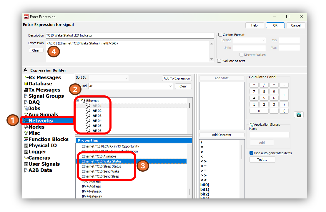
After selecting the control, and opening the Expression Builder , the following steps will bind the value of one of the TC10 properties to that control.
 Select the Networks in the left pane.
 Select one of the Automotive Ethernet networks as the source of the status. (In this case AE 01 is chosen)
 In the properties pane, scroll down to the TC10 commands shown in the diagram above.
 Adding this property to the expression will bind its value to the control.
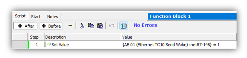
Sending TC10 Commands from a Function Blocks
Function Blocks are scripts created in Vehicle Spy. The TC10 status of an Ethernet port can be referenced using the same interface as used for Graphical Panels and it can be used in the logical statements of a script. The TC10 sleep and wake requests can also be sent by using Function Blocks using the Set Value Command as shown below.
More info on the Function Blocks and their editor can be found in this section of the Vehicle Spy documentation.
The Set Value Command uses the same Expression Builder interface to write a value to a property.
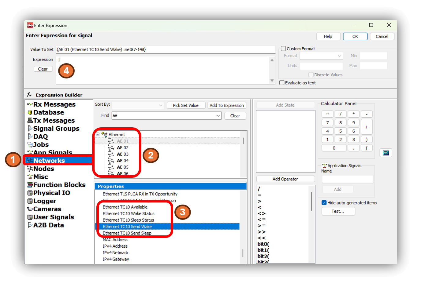
From this screen follow steps similar to the last example.
Select the Networks in the left pane.
Select an Automotive Ethernet networks to send the TC10 command. (In this case AE 01 is chosen)
In the properties pane, scroll down to the TC10 commands shown in the diagram above.
Select this Send Wake or Send Sleep property
as the value to set, and set the expression to 1.
3.5.2. Using TC10 with Intrepid’s Open Source APIs
libicsneo is the Intrepid Control Systems device communication library.
Installation and usage documentation can be found within each of the respective APIs.
TC10 C++ API
Download this C++ TC10 Example
to see the use of the following C++ functions.
TC10 Python API
Following are the equivalent TC10 functions for Python.
TC10 C API
Coming Soon!
TC10 is not supported in Intrepid legacy APIs
There is no support for TC10 in the neoVI API (icsneo40) or python_ics. Please consider using libicsneo or Vehicle Spy 3 .
If you are having trouble working with TC10 using any of the interfaces above, please contact our Customer Support
3.6. MACsec
MACsec (802.1AE) is a Layer 2 protocol that can ensure data integrity and authenticity, as well as data encryption. The OPEN Alliance TC17 has drafted the MACsec Automotive Profile to adapt the broad standards of 802.1AE to automotive applications.
The use and operation of MACsec is well beyond the scope of this guide, but many Intrepid products contain Automotive Ethernet PHYs with MACsec support. This guide explains the different way of loading MACsec configurations and keys into the Automotive Ethernet PHY.
3.6.1. Intrepid Devices Supporting MACsec
The MACsec configuration of a PHY is contained in a yaml file that is sent to the PHY Using Vehicle Spy or one of Intrepid’s API. (Examples follow) The following table contains the information needed to address the PHY using the API.
Product |
Serial # |
Port |
netid |
config_netid |
RAD-Moon2_zl |
RNxxxx |
100/1000BASE-T1 |
NETID_OP_ETHERNET1 |
NETID_MDIO_01 |
RAD-Moon3 |
R3xxxx |
100/1000BASE-T1 |
NETID_OP_ETHERNET1 |
NETID_MDIO_01 |
RAD-Comet2 |
RCxxxx |
AE01 |
NETID_OP_ETHERNET1 |
NETID_MDIO_02 |
|
GSxxxx |
SFP1 |
NETID_ETHERNET |
NETID_I2C1 |
SFP2 |
NETID_ETHERNET2 |
NETID_I2C2 |
||
RAD-Galaxy2 |
AE01 |
|||
AE02 |
||||
AE03 |
||||
AE04 |
||||
AE05 |
||||
AE06 |
||||
AE07 |
||||
AE08 |
||||
AE09 |
||||
AE10 |
||||
AE11 |
||||
AE12 |
||||
AE13 |
||||
AE14 |
||||
AE15 |
||||
AE16 |
3.6.2. Configuring MACsec in Vehicle Spy 3
In Development
3.6.3. Configuring MACsec using Intrepid’s Open Source API
libicsneo is the Intrepid Control Systems device communication library.
Installation and usage documentation can be found within each of the respective APIs.
MACsec C++ API
Coming Soon!
MACsec Python API
Coming Soon!
MACsec C API
Coming Soon!
3.6.4. Configuring MACsec in using python_ics
Python Installation
pip install python_ics pyyaml
Usage
ics_load_macsec.py [-h] [--yaml YAML] --port PORT [--reset] serial_number
serial_number
The serial number of the device to configure.
options
Option |
Descrition |
Default Value |
-h, –help |
show this help message and exit |
|
–yaml YAML |
filename of yaml configuration to be loaded (Assumes .yml is located in “/yaml/” directory) |
test_macsec_Rule_wildcard_SecY_128_strip_strict_sci_SA_sak0.yml |
–port PORT |
‘config_netid’ - network ID for the port configuration network. |
config_netid = NETID_I2C2 |
‘netid’ - network ID for the port network. |
netid = NETID_OP_ETHERNET1 |
|
–reset |
Reset and clear and disable MACsec on the device, then exit; yaml configuration ignored |
FALSE |
Example Command Lines
RAD-Comet2:
python ics_load_macsec.py RCxxxx --port "{'netid':NETID_OP_ETHERNET1,'config_netid':NETID_MDIO_02}" --yaml "test_sfp_macsec_Rule_wildcard_SecY_128_strip_strict_sci_SA_sak0.yml"
RAD-Moon2_zl:
python ics_load_macsec.py RNxxxx --port "{'netid':NETID_OP_ETHERNET1,'config_netid':NETID_MDIO_01}" --yaml "test_sfp_macsec_Rule_wildcard_SecY_128_strip_strict_sci_SA_sak0.yml"
RAD-Moon3:
python ics_load_macsec.py R3xxxx --port "{'netid':NETID_OP_ETHERNET1,'config_netid':NETID_MDIO_01}" --yaml "test_sfp_macsec_Rule_wildcard_SecY_128_strip_strict_sci_SA_sak0.yml"
RAD-Gigastar Port1 with SFP-MV2221M:
python ics_load_macsec.py GSxxxx --port "{'netid':NETID_ETHERNET,'config_netid':NETID_I2C2}" --yaml "test_sfp_macsec_Rule_wildcard_SecY_128_strip_strict_sci_SA_sak0.yml"
RAD-Gigastar Port2 with SFP-MV2221M:
python ics_load_macsec.py GSxxxx --port "{'netid':NETID_ETHERNET2,'config_netid':NETID_I2C3}" --yaml "test_sfp_macsec_Rule_wildcard_SecY_128_strip_strict_sci_SA_sak0.yml"